
As 800G and even 1.6T optical modules are deployed at an accelerating pace inside AI data centers, demand for indium phosphide (InP) substrates, the core material for photonic chips, continues to climb. Multiple upstream material suppliers report that their order visibility for 2026 already extends into the second half of the year, and the supply gap remains wide. Domestic InP crystal growth and supporting equipment localization is speeding up markedly.

Why AI Optical Modules Depend on InP
Indium phosphide has a direct bandgap, high electron mobility, and lattice-matching with InGaAs and InAlAs epitaxy, which makes it the preferred substrate for DFB lasers, EML electro-absorption modulated lasers, and coherent photodetectors. An 800G module integrates dozens or even hundreds of photonic chips, and the 1.6T generation places far stricter requirements on substrate flatness, dislocation density, doping uniformity, and surface particles. In AI compute clusters that ship tens of thousands of GPUs, optical module volumes are multiplied many times over, and that demand is transmitted directly to upstream substrates.
Supply Gap and Domestic Capacity Ramp
Global InP substrate capacity is concentrated in a small number of overseas suppliers. Chinese producers grow InP crystals using the vertical gradient freeze (VGF) method and are gradually moving 2-inch, 3-inch, and 4-inch substrates into mass production. Constrained by boule size, yield, and qualification cycles, domestic InP substrates cannot fully satisfy the explosive demand from optical modules in the short term, keeping prices high. Industry consensus holds that the supply gap will remain above seventy percent in 2026, and capacity expansion is the main theme, with photonic chip makers signing long-term supply agreements to lock in capacity.
Technology Trend: Larger Size and Higher Uniformity
To lower the cost per photonic chip, InP substrates are evolving from 2 inches toward 3 and 4 inches; the larger the epitaxial wafer, the more chips can be processed per wafer. At the same time, requirements on micropipes, dislocations, and impurities continue to tighten in order to lower laser threshold current and failure rates. This raises the bar for growth furnace temperature control, slicing, and back-end cleaning equipment.
Photonic Chip Types That Depend on InP
Inside an optical module, InP-based platforms support several key devices: distributed feedback (DFB) lasers for direct-detection links, electro-absorption modulated lasers (EMLs) for longer-reach and higher-rate links, and avalanche photodiodes (APDs) and coherent detectors for high-sensitivity reception. Each of these devices is grown epitaxially on an InP substrate, so the quality and uniformity of that substrate directly sets the yield of the photonic chip. As module line rates move from 100G per lane toward 200G and beyond, the tolerance for substrate defects narrows further, and manufacturers increasingly specify tighter dislocation and particle limits. This is why substrate qualification has become a bottleneck that cannot be solved overnight.
Supply Chain Dynamics and Pricing
The global InP substrate market has historically been served by a small number of Japanese, European, and U.S. suppliers, with long lead times and tight allocation. As AI cloud providers race to deploy bandwidth-dense clusters, optical module makers have been forced to secure InP supply months in advance, and spot premiums have widened. Chinese substrate producers, while still smaller by volume, are improving crystal diameter, yield, and defect metrics through VGF growth and refined polishing. Their ability to offer shorter lead times and localized technical support is gradually winning design sockets, even if the high-end coherent segment remains dominated by incumbents for now.
Outlook for InP Demand
Looking ahead, AI compute buildout remains in a high-growth phase, and the upgrade from 800G to 1.6T modules will continue to pull InP substrate demand. Domestic progress in VGF InP growth, substrate processing, and precision cleaning will determine whether Chinese substrates can capture a larger share of this optical module expansion. Localized equipment not only lowers line investment but also provides fast, customized support during process iteration, helping substrate makers respond quickly to photonic chip customer specifications. Whoever can lead in substrate yield and delivery lead time will gain an edge in the coming supply-chain competition. For Chinese producers, the combination of surging domestic optical module demand and a policy push toward self-reliance creates a rare window to move from niche supplier to qualified volume partner. Success will depend not only on crystal growth but also on the downstream cleaning and handling steps that determine whether a grown crystal becomes a shippable, specification-compliant wafer. For Chinese InP producers, the current demand surge is both an opportunity to scale revenue and a forcing ground to improve quality, since customers will only commit to long-term supply if yield and consistency meet their standards.
The Role of Substrate Quality in Photonic Yield
Even a handful of dislocations or particles per square centimeter can degrade laser threshold current and accelerate failure in photonic chips, so InP substrate quality directly translates into module yield. Substrate suppliers must tightly control crystal composition, doping uniformity, and post-processing surface finish. The move to larger wafers amplifies these challenges because it is harder to hold uniformity across a 3- or 4-inch diameter than a 2-inch one. Domestic InP makers invest in VGF process control, slicing, and multi-step cleaning to meet these tighter specs, and the availability of dedicated cleaning equipment is often the deciding factor between a substrate that meets customer specs and one that must be scrapped.
The Opportunity for Domestic Cleaning Equipment
Indium phosphide is relatively soft and sensitive to acids and alkalis, so its cleaning and processing differ substantially from silicon wafers. Hebei Zhongke Microelectronics Co., Ltd. has developed a semi-automatic single-wafer cleaning machine for InP back-end processes (model SQX-150-5Y1D, the InP cleaning machine), alongside a VGF crystal growth furnace, a wafer unloading table, and a single-wafer cleaning and spin dryer. These products support InP crystal and epitaxy makers with a coordinated line spanning crystal growth, wafer unloading, precision cleaning, and spin drying, helping domestic InP substrate capacity ramp up steadily and reduce reliance on imported cleaning equipment.
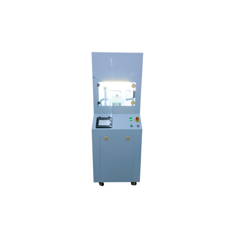
Against the backdrop of sustained AI compute growth, the window for domestic substitution of InP substrates and their growth and cleaning equipment is wide open. For inquiries about the InP cleaning machine, VGF crystal growth furnace, and related solutions, call the consultation hotline: 17177768881.