
Domestic 12-inch semiconductor wafer capacity is ramping up steadily. Several large wafer makers report that new-line yields and shipments are improving month by month, and domestic 12-inch polished and epitaxial wafers have entered mainstream wafer fabs in volume, providing key material support for Chinese fab expansion.
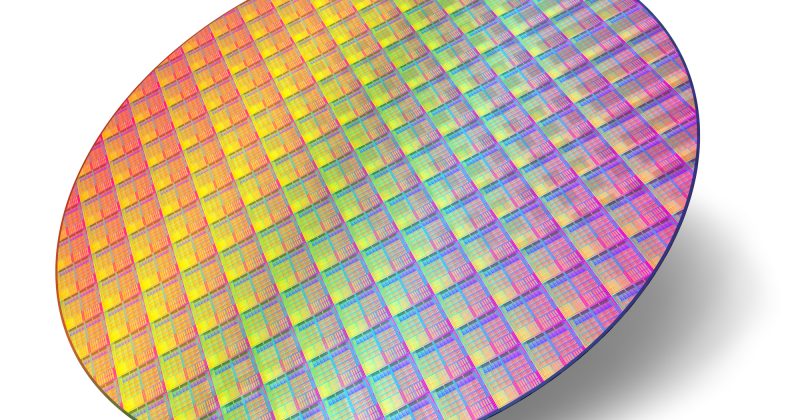
Large Wafers Are the Bedrock of Fabs
Twelve-inch (300 mm) wafers are the mainstream substrate for advanced logic and memory manufacturing. A single 12-inch wafer yields hundreds of chips, and each step up in diameter roughly doubles die output. For a long time, the high-end 12-inch wafer market was dominated by a few overseas suppliers. After more than a decade of investment, Chinese makers have broken through in pulled single crystal, slicing, grinding, polishing, and epitaxy, and now supply from mature to more advanced process nodes.
Capacity Ramp and Customer Qualification
Several domestic 12-inch lines are in yield ramp, covering polished wafers, epitaxial wafers, and bonded SOI-type material. As Chinese fabs keep expanding, the share of locally sourced large wafers is rising. Makers keep improving particle control, flatness, and metal contamination, passing automotive and industrial customer qualifications, and their order mix is shifting from low-end toward high-end products. Some are also pushing 14 nm and below logic wafer qualification.
Customer Mix Upgrading
Domestic 12-inch wafers are extending from mature toward advanced nodes. Early domestic polished wafers mainly served power management and display drivers; as flatness, particle, and metal contamination metrics improved, they have gradually entered logic, memory, and automotive-grade supplier lists. Some makers’ epitaxial wafers are already supplied in volume into specialty and power device lines. Fabs, motivated by supply-chain security, are actively cultivating second and third domestic suppliers, giving wafer makers steady qualification orders and expansion momentum.
From Pulled Crystal to Polished Wafer
The journey from polysilicon to a finished 12-inch wafer is long: Czochralski pulling of single-crystal ingots, axial and radial resistivity control, diamond-saw slicing, edge grinding, lapping, etching, chemical-mechanical polishing, and final cleaning. Each step must hold extremely tight tolerances on total thickness variation, bow, warp, and surface microroughness. Domestic makers have invested heavily in the entire flow rather than a single step, which is why their wafers now meet fab specifications for particle counts below tight thresholds and metal contamination at parts-per-billion levels. The cumulative effect of process discipline across all these steps is what allows a wafer maker to move from sampling to volume supply.
Demand Drivers and Import Substitution
Chinese fabs have continued to add capacity across mature, specialty, and automotive-grade logic and power, all of which consume 12-inch wafers. Because wafer fabs prefer to qualify multiple suppliers to de-risk their supply chain, domestic makers are naturally positioned to win second-source and third-source slots. Even where advanced leading-edge logic still relies on imported wafers, domestic polished and epitaxial wafers are gaining share in power management, image sensors, display drivers, and embedded memory. As capacity utilization normalizes, the focus shifts from volume to yield and cost, which favors makers who have paired wafer production with localized back-end equipment support.
Outlook for Large-Wafer Localization
Looking ahead, domestic 12-inch wafers will keep raising self-sufficiency in mature and selected advanced nodes. As Chinese fabs expand and logic, memory, and power demand recover, large-wafer demand should grow steadily. During capacity expansion, wafer makers demand ever higher cleanliness, automation, and reliability from single-wafer cleaning and spin drying equipment. Domestic equipment firms that deliver stable, reliable solutions for large-wafer handling will form a virtuous cycle with large-wafer ramp-up, jointly supporting supply-chain self-reliance. The transition from 6-inch and 8-inch to 12-inch also raises the bar on every back-end step, which favors equipment suppliers who keep pace with wafer size trends. Larger wafers are thinner per unit area and more prone to breakage, so handling, cleaning, and spin drying must be gentler and more precise. Domestic equipment makers that engineer tools specifically for 12-inch wafers, rather than scaling up older designs, are better positioned to win qualification at large wafer makers and fabs alike. As domestic 12-inch capacity continues to ramp, the focus will shift from simply producing wafers to producing them consistently and cost-effectively, which raises the importance of every back-end step. Equipment that improves yield and reduces breakage will be rewarded with recurring orders. As domestic wafer share rises, the strategic value of a stable domestic back-end equipment supply chain grows, because fabs and wafer makers cannot risk production bottlenecks from imported tools with long lead times. This operational resilience, rather than headline price alone, is increasingly what wafer makers weigh when selecting their back-end equipment partners.
Specifications That Fabs Care About
When fabs qualify a 12-inch wafer supplier, they measure parameters such as total thickness variation, local and global flatness, bow and warp, surface particles at multiple size thresholds, metal contamination, and oxygen and carbon content. Each of these metrics must be held within tight bounds across an entire production lot, because a single out-of-spec wafer can disrupt an expensive lithography or deposition run. Domestic wafer makers have invested in metrology and process control to demonstrate lot-to-lot consistency, not just one-off good samples. This consistency is what turns a qualified sample into a standing production order, and it depends heavily on stable back-end cleaning and drying steps that do not introduce new particles or water marks.
Back-End Cleaning and Drying Equipment Localizes in Step
Large, thin 12-inch wafers place higher demands on single-wafer cleaning and spin drying. Hebei Zhongke Microelectronics Co., Ltd. has developed a 12-inch wafer spin dryer and single-wafer cleaning and spin dryer (model SG-8-12-2D), along with a fully automatic single-wafer cleaning machine and a wafer unloading table. These products provide high-purity single-wafer cleaning, centrifugal spin drying, and automated wafer unloading for large wafer makers and fabs, reducing particle residue and water-mark defects and supporting steady domestic wafer capacity ramp. The equipment accommodates 6, 8, and 12-inch wafers to flexibly serve different lines.
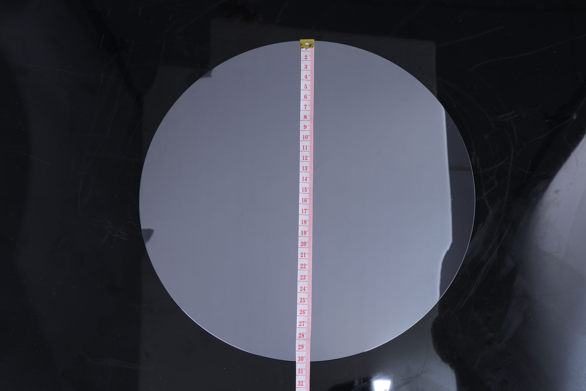
Large-wafer localization is a long road, and coordinated localization of back-end cleaning and drying equipment is equally important. For inquiries about the 12-inch wafer spin dryer, single-wafer cleaning machine, and wafer unloading table, call the consultation hotline: 17177768881.