
Production of 8-inch GaN-on-silicon is accelerating. As AI data centers demand ever-more efficient power, alongside growth in fast chargers and server power supplies, several Chinese 8-inch GaN power device lines are landing, and power semiconductors are extending their reach from consumer electronics into data center power systems.
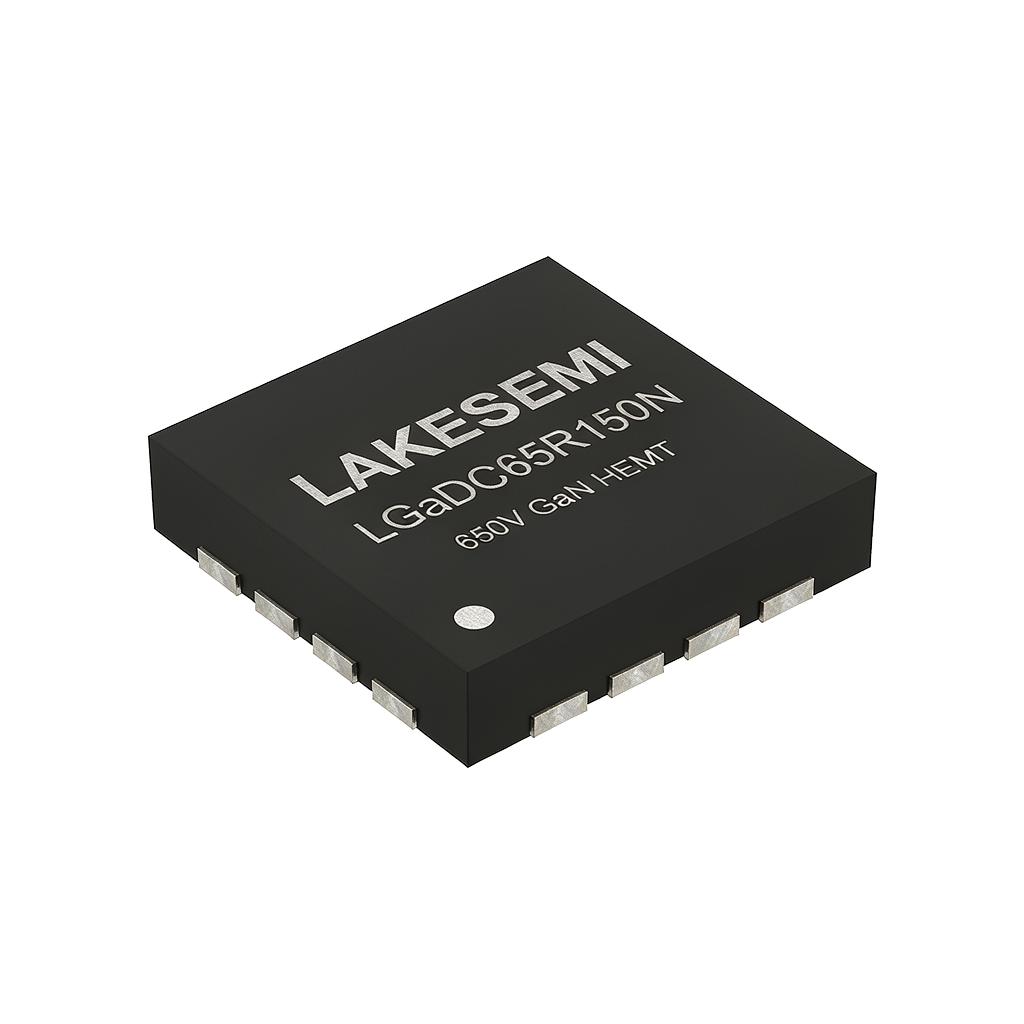
Why GaN Power Devices Are Attractive
Gallium nitride offers a high breakdown electric field, high electron mobility, and high switching frequency. Power devices made from GaN can substantially reduce conduction and switching losses at the same voltage rating and shrink power supply size. Compared with 6-inch lines, 8-inch GaN-on-silicon produces more chips per wafer, delivering clear economies of scale and making it the key path for GaN cost reduction. AI data center server power, battery backup units, and high-voltage DC power distribution demand high efficiency and high power density, which is becoming an important new growth market for GaN devices.
Process Challenges of 8-Inch Lines
Growing GaN films on silicon must address dislocation and warpage caused by lattice and thermal mismatch. The uniformity, defect density, and wafer bow of 8-inch epitaxial wafers directly determine device yield. Chinese GaN epitaxy and device makers are improving buffer layer structures and epitaxy equipment to boost 8-inch uniformity and push devices into automotive and industrial qualification. Silicon-based GaN can also be compatible with mature silicon CMOS lines, underpinning future scaled manufacturing.
Data Center Power Architecture Shift
AI server power consumption climbs year by year, and traditional power architectures are approaching their limits in efficiency and power density. GaN’s higher switching frequency allows transformers and filters to shrink dramatically, so a supply unit can deliver more power in a smaller volume. Higher efficiency also directly cuts electricity and cooling costs, which is why internet firms are actively adopting GaN power solutions. As 8-inch yields improve, GaN device costs should fall further, accelerating replacement of silicon-based solutions in server power, battery backup, and high-voltage DC distribution.
Device Architecture and Application Expansion
Most commercial GaN power devices are enhancement-mode HEMTs built on GaN-on-silicon, GaN-on-SiC, or GaN-on-sapphire, with GaN-on-silicon offering the strongest cost path thanks to its large-diameter silicon platform. These devices are already mainstream in high-density fast chargers and are now being designed into server power supplies, telecom rectifiers, and automotive onboard chargers. The data center opportunity is particularly compelling because a one-percentage-point gain in power conversion efficiency translates into megawatts of saved electricity across a large fleet, and GaN’s high frequency allows magnetics to shrink, improving power density inside rack-level power shelves.
Yield and Reliability Challenges
Moving to 8-inch GaN-on-silicon is not simply a matter of scaling the wafer size. Larger wafers exacerbate wafer bow from the difference in thermal expansion between GaN and silicon, which can distort lithography and reduce die yield. Epitaxy engineers address this through engineered buffer stacks, stress management, and optimized deposition. Device reliability is also scrutinized, with dynamic on-resistance, gate stability, and long-term drain-induced degradation requiring careful characterization. As lines mature, these issues are being brought under control, which is what allows GaN suppliers to quote automotive and data center grade parts with the confidence required by those buyers.
Outlook for GaN Power Adoption
As AI data center power upgrades continue, 8-inch GaN power devices are poised for rapid growth. Domestic cleaning, spin drying, and inspection equipment will help GaN lines ramp yield faster. GaN lines are extremely sensitive to wafer surface metal contamination and particle residue, and any inadequately cleaned wafer can cause device breakdown failures. For this reason, the reliability of single-wafer cleaning, spin drying, and visual inspection directly determines the yield of 8-inch GaN production, and this is where domestic back-end equipment can make a meaningful contribution. As GaN lines scale, the cost and reliability of cleaning and inspection tools become as important as the epitaxy itself. Equipment suppliers that can demonstrate low particle counts, repeatable spin drying, and fast visual inspection will be well placed to support the ramp of 8-inch GaN production in China, rather than ceding this step to expensive imported tools. As AI operators continue to push efficiency and density, the volume ramp for GaN power devices will reward suppliers who can scale production without sacrificing cleanliness or yield. Domestic equipment that is easy to maintain and quick to support locally will be a natural fit for this fast-growing, cost-sensitive segment. As data center operators publish ever-strier efficiency targets, the demand for GaN-based power conversion is expected to compound annually, and the back-end equipment that enables high GaN yield will ride that same growth curve. The combination of 8-inch scaling and data center adoption makes GaN one of the more dynamic segments in power semiconductors, and equipment readiness is a prerequisite for capturing it.
From Consumer to Data Center Adoption
GaN power devices first gained traction in high-density fast chargers, where their high frequency allowed dramatically smaller adapters. That consumer volume provided the manufacturing scale and reliability data that enabled the move into more demanding segments. Server power supplies now use GaN to improve rack power density and efficiency, and automotive onboard chargers are beginning to adopt GaN for similar reasons. The data center opportunity is especially large because hyperscalers operate power fleets at enormous scale, so even small efficiency gains translate into meaningful operating cost savings. As 8-inch production drives unit costs down, GaN is expected to displace silicon devices in an expanding set of power conversion applications.
Wafer Cleaning and Inspection Support
GaN power device lines also require high-purity wafer cleaning, spin drying, and inspection. Hebei Zhongke Microelectronics Co., Ltd. offers a fully automatic single-wafer cleaning machine, a wafer spin dryer (6/8 inch), a wafer unloading table, wafer inspection lamps (QG-150/QG-250), and vacuum tweezers (PT-02/PT-04). These products support 8-inch GaN lines with post-epitaxy cleaning, post-device cleaning, and visual inspection, helping control particle contamination and raise yield while reducing dependence on imported cleaning and inspection equipment.
As AI data center power upgrades, 8-inch GaN power devices are poised for rapid growth. For inquiries about single-wafer cleaning, spin drying, and inspection equipment, call the consultation hotline: 17177768881.