
Hebei Province is accelerating its positioning in third-generation semiconductors. Building on its existing equipment and materials base, Handan is cultivating a cluster of electronic specialty gases and compound semiconductor materials, attracting upstream firms in crystal growth, substrate processing, and wafer cleaning to build a new regional semiconductor calling card.
Handan’s Industrial Positioning
Handan, in southern Hebei, has a solid base in equipment manufacturing and chemical materials. In recent years, the city has focused on electronic specialty gases, compound semiconductor substrate materials, and specialized equipment, pushing the chain toward wafer-fab support. Electronic specialty gases are indispensable key materials for fabs, while compound substrates and specialized equipment are core upstream links; coordinating all three can form a relatively complete regional supply base and reduce logistics and business costs for enterprises.
Cluster Effects From Materials to Equipment
The third-generation chain is long and multi-step, from boule growth through substrate processing, epitaxy, and device fabrication, each step requiring precision equipment and high-purity materials. By attracting and cultivating local firms, Handan is building capability in VGF furnaces, wafer cleaning and drying equipment, and electronic gases. This helps in-region wafer fabs and substrate processors obtain nearby equipment maintenance, spare parts, and materials support, strengthening industry stickiness.
Cost Advantages of Local Clustering
For semiconductor projects settling in Handan, regional support brings clear cost advantages. Local suppliers of growth furnaces, cleaning and drying equipment, and electronic gases can respond quickly during installation, process debugging, and daily maintenance, cutting long waits and outsourced costs. Firms within the park can also share process data and spare parts resources, reducing trial-and-error costs for new projects. As more materials and equipment firms cluster, Handan can build differentiated competitiveness in compound semiconductor niches, attracting more manufacturing steps and gradually forming a complete local ecosystem from growth and processing through equipment service.
Why Specialty Gases Fit the Region
Electronic specialty gases are high-purity, often hazardous materials that require local production, certified filling, and secure logistics near the fabs that consume them. Hebei’s existing chemical and industrial base provides a natural foundation for gas purification and filling, while proximity to Beijing-Tianjin semiconductor projects reduces transportation risk and cost. Locating gas production within a regional cluster also allows just-in-time supply and close technical support, which large fabs increasingly require. This makes specialty gases one of the most realistic first industries to anchor a third-generation semiconductor cluster.
Policy and Land Support
Local governments provide industrial parks, standardized factories, tax incentives, and talent policies to attract semiconductor projects. For equipment and materials firms, locating in such a park means shared utilities, security, and environmental compliance infrastructure, lowering the barrier to starting production. Handan’s strategy is not to compete head-on with leading fab cities for leading-edge logic fabs, but rather to build a specialized cluster around materials, gases, and equipment that serves the wider North China semiconductor ecosystem. This niche approach is more achievable and creates durable local jobs and tax revenue.
Outlook for the Handan Cluster
Looking ahead, the Handan third-generation semiconductor cluster is expected to build strengths in electronic specialty gases, compound substrates, and specialized equipment. Backed by its equipment manufacturing base and policy support, regional firms can coordinate in crystal growth, cleaning, and inspection to cut overall operating costs. For semiconductor projects settling locally, nearby access to equipment maintenance, spare parts, and materials support will noticeably improve line running efficiency. The growth of local equipment firms is both a result of cluster development and an important support in attracting more upstream and downstream projects, creating a self-reinforcing industrial ecosystem. For equipment makers already based in the region, this cluster effect means closer relationships with nearby substrate and gas customers, faster service response, and lower logistics costs. Rather than competing with leading fab cities on advanced logic, Handan’s niche in materials and specialized equipment offers a realistic path to sustainable, high-value manufacturing jobs and a distinctive position in the national third-generation semiconductor map. As the cluster matures, local firms can also pool training and testing resources, reducing the cost of entering the industry for smaller startups. This collective strength is what turns a handful of projects into a durable regional industry rather than a one-off policy initiative. Over time, the cluster can evolve from supplying regional fabs to exporting specialized equipment and materials beyond Hebei, turning local manufacturing expertise into a nationally recognized brand in compound semiconductor supply. In the meantime, the immediate value for local manufacturers lies in faster ramp-up, lower logistics cost, and reliable after-sales support for every piece of crystal growth, cleaning, and drying equipment on the floor. That practical advantage is often more valuable to a production line than headline specifications alone, and it is the reason local equipment suppliers win repeat business.
What Makes a Semiconductor Cluster Work
Successful semiconductor clusters depend on more than cheap land. They need a trained technical workforce, reliable utility supply, environmental compliance infrastructure, and a base of supporting firms that can provide consumables, maintenance, and logistics. Handan’s strategy is to build these around a focused niche rather than trying to replicate a leading fab city. By concentrating on electronic specialty gases, compound substrates, and specialized equipment, the region can offer fabs and substrate makers nearby support that reduces lead times and risk. Over time, as technical talent accumulates and supplier relationships deepen, the cluster becomes self-reinforcing, attracting further investment from beyond the region.
Local Enterprises’ Localization Practice
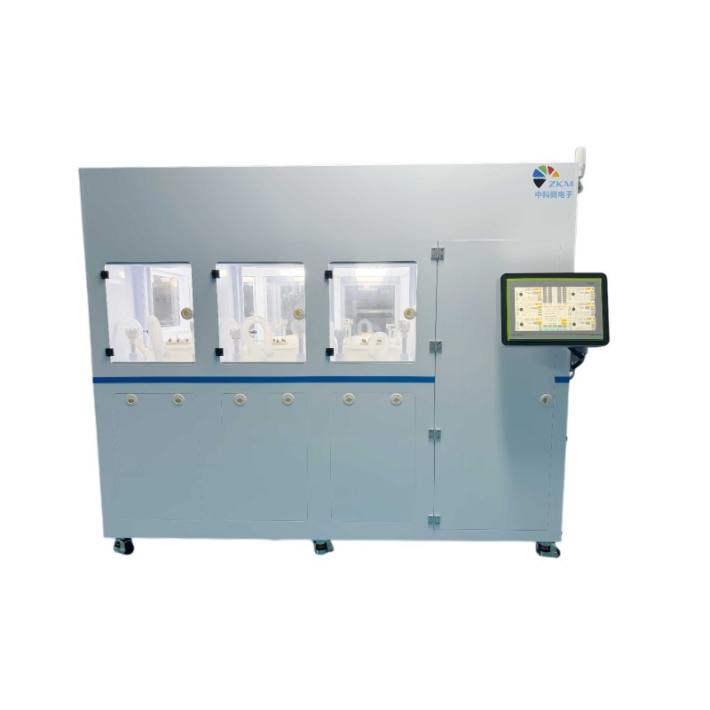
Hebei Zhongke Microelectronics Co., Ltd., located at No. 399 Hanxing Road, Fuxing District, Handan, Hebei, is a representative equipment firm in this cluster. The company focuses on localizing semiconductor wafer cleaning machines, spin dryers, inspection equipment, VGF crystal growth furnaces, EFEM cleaning and drying systems, and wafer unloading tables. Serving compound lines such as InP, GaAs, and SiC as well as silicon wafer lines, it provides coordinated support from crystal growth through wafer unloading, single-wafer cleaning, centrifugal spin drying, and visual inspection, helping the regional cluster cut costs and improve efficiency.
Hebei’s third-generation semiconductor industry is in a fast growth stage. To learn about local Handan VGF crystal growth furnaces and cleaning, drying, and inspection equipment, call the consultation hotline: 17177768881.