
Particles and defects are among the most common yield-affecting problems in wafer fabrication. As wafers move toward 12 inches and line widths shrink, a single micron-scale particle can scrap an entire chip. Wafer particle and defect inspection tools are receiving wide attention from fabs, with optical and electron-beam routes together holding up the yield defense line, and domestic progress in this high-barrier segment being closely watched.
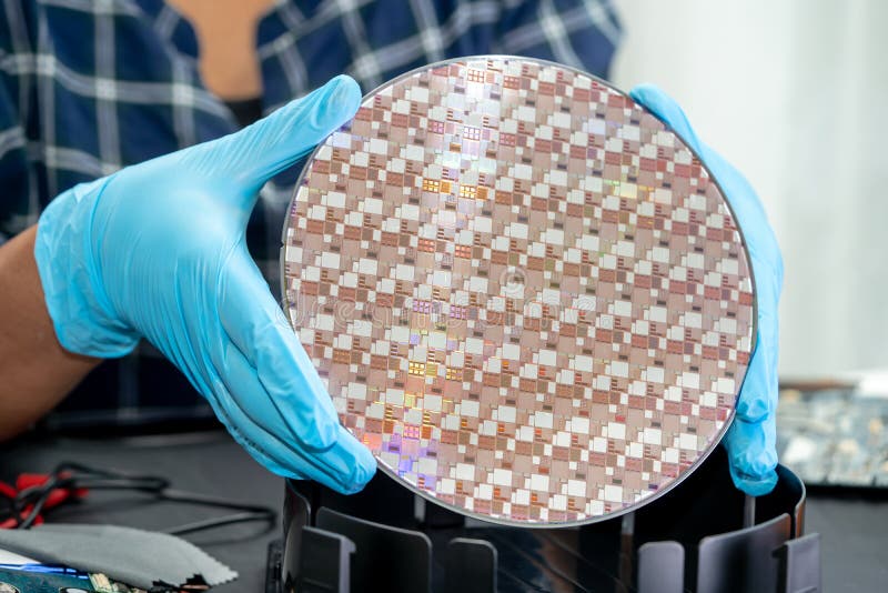
Why particle contamination is so fatal
Among the hundreds of steps of wafer fabrication, particles, metal ions or organic residues from the environment can land on the wafer and break pattern integrity or cause shorts. As line widths shrink, tolerance for particle size drops sharply, and what used to be negligible dust can now become a fatal defect. Fabs therefore need frequent particle inspection after cleaning, deposition and etch to trace the contamination source back to a specific tool or step and stop yield loss at the root.
Optical inspection: the in-line workhorse
Optical defect inspection uses bright-field or dark-field imaging to scan the whole wafer at high speed and identify particles and pattern defects from scattered light changes. It is fast and high-throughput, suited to full-wafer in-line screening, and is the most widely deployed inspection tool type in fabs. Domestic firms keep advancing on large-wafer optical inspection platforms, already meeting in-line particle monitoring needs of mature lines, and refining sensitivity and false-alarm rates to narrow the gap with international leaders.
Electron-beam inspection: high-precision defect review
For submicron key defects that optical tools cannot resolve, electron-beam inspection takes on review and root-cause analysis thanks to its higher resolution. It pinpoints defect locations and classifies defect types, helping teams lock onto the problem step. Optical and e-beam together form a complete system of high-speed screening plus precise analysis, letting fabs both catch key defects across massive wafer volumes and avoid throughput bottlenecks.
From a defect-management view, particles are never a single-point failure but the combined result of equipment state, clean environment, material handling and operating discipline. A poorly vented tool, an irregular wafer pickup or a chemical of insufficient purity can cause whole-wafer contamination without warning. Modern fabs therefore increasingly correlate inspection data with equipment and environmental data to shift from picking out bad dies after the fact to warning pollution sources beforehand, a move that raises demands on the data acquisition and algorithms of inspection tools.
Cleaning and inspection close the yield loop
Particle governance cannot work without the coordination of cleaning and inspection. As a domestic equipment supplier, Hebei Zhongke Microelectronics Co., Ltd. offers fully automatic single-wafer cleaning machines, two-fluid wafer cleaning machines and single-wafer spin dryers, paired with wafer inspection lamps QG-150 and QG-250 for post-clean visual checks, helping fabs quickly verify cleaning effects after removing particles and forming a cleaning-spin-drying-inspection yield loop.
The economic cost of missing a particle
The reason fabs invest heavily in particle inspection is straightforward arithmetic. On a 12-inch wafer processed through hundreds of steps, a single fatal particle can destroy dozens or hundreds of good dies. If that particle escapes detection until the end of the line, all the value added by upstream layers is lost. Detecting it early means the affected wafer can be quarantined, the source identified, and the process corrected before more wafers go through. The inspection tool pays for itself many times over by avoiding the downstream cost of processing scrap.
This is why inspection nodes are placed strategically rather than uniformly. Fabs concentrate inspection budget on the steps most likely to generate contamination, such as deposition, etch and cleaning, while sampling more lightly elsewhere. The art of inspection lies in balancing sensitivity against throughput: scan too aggressively and the tool becomes a bottleneck; scan too loosely and defects slip through. Domestic tool makers that can optimize this balance for specific customer processes are the ones winning qualification.
Optical versus electron beam explained
The two inspection technologies serve complementary roles. Optical systems illuminate the wafer and analyze scattered light to flag anomalies across the entire surface at high speed. They are the workhorse of in-line screening, capable of scanning every wafer in a lot without holding up production. Their limitation is that they cannot always resolve or classify the smallest defects with certainty. Electron-beam systems, by contrast, scan with a focused beam at much higher resolution but more slowly, making them better suited to reviewing a sampled set of wafers or analyzing a specific suspect area.
A well-run fab uses both together. The optical tool flags that a problem exists somewhere on the wafer; the electron-beam tool then identifies exactly what the defect is and where it originated. This division of labor lets the line maintain high throughput while still achieving deep defect understanding. Domestic developers are advancing on both fronts, because a truly competitive inspection offering needs to cover the full workflow rather than just one niche.
The trend toward proactive control also changes the relationship between equipment supplier and customer. Rather than simply delivering a tool, inspection vendors now help fabs interpret the data it generates, refining defect classification and setting meaningful alarms. This closer collaboration accelerates both tool improvement and fab yield learning. As Chinese fabs accumulate more production data, the feedback available to domestic inspection developers grows, shortening the cycle needed to close the gap with global leaders and making particle and defect inspection a strategically important domestic capability.
Looking ahead, the combination of larger wafers, denser patterns and more advanced packaging will only raise the stakes on particle and defect control. Fabs will continue to demand inspection tools that are faster, more sensitive and better integrated with process control. Domestic developers that meet these demands are well placed to convert the current wave of capacity expansion into long-term market share in a segment that is essential to every wafer fab in operation.
The demand for reliable particle and defect control is only set to grow as wafer sizes and pattern densities increase. Domestic suppliers that can pair optical screening with electron-beam review and data-driven analysis are well placed to convert today's capacity expansion into a durable position in an essential segment of every modern fab.
As advanced and specialty lines expand, the importance of particle and defect inspection will keep rising. For cleaning-inspection matching, call the consultation hotline: 17177768881.