
With the most advanced nodes hard to push further, Chiplet and heterogeneous integration have become an important path to sustain performance gains. By packaging different small chips together, systems can achieve higher integration without chasing the leading edge. Recently, domestic advanced packaging line expansion has cumulatively exceeded 20 billion RMB, with Chiplet and 2.5D/3D packaging becoming a focus of capital and industry, and dragging along a whole set of dedicated packaging equipment.
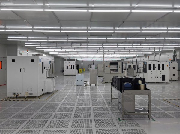
Why Chiplet became a breakthrough
When the cost and difficulty of shrinking a single chip to the leading edge rise sharply, splitting the large die into multiple chiplets and interconnecting them densely through advanced packaging becomes an accepted cost-effective route. Chiplets let different functions and nodes play to their strengths, cutting manufacturing cost while improving design flexibility. The hunger for compute and bandwidth from AI, high-performance computing and automotive chips is accelerating this trend, moving packaging from a back-end supporting role to a star of system performance.
Domestic lines expand beyond 20 billion RMB
Responding to this trend, domestic OSATs and fabs are adding advanced packaging capacity. Investment around 2.5D, 3D packaging, through-silicon vias (TSV) and wafer-level packaging keeps landing, with total expansion topping 20 billion RMB. At the same time, demand for bonding, dicing, temporary bonding and debonding, and package-level inspection is pulled up, opening new space for domestic equipment. Some firms that previously focused on front-end equipment are also extending product lines into advanced packaging.
From the industrial logic, the rise of advanced packaging is essentially an inevitable search for cost-effective paths when leading-edge shrinks become uneconomic. As large die splitting and repacking lowers cost, the trend benefits not only OSATs but also pulls a batch of front-end equipment makers into bonding, temporary bonding and debonding, wafer thinning, package-level cleaning and inspection. China is building lines while filling gaps in equipment, materials and standards, and a complete ecosystem from chiplet design and wafer-level packaging to test is taking shape.
Pre-packaging cleaning and wafer handling benefit too
Advanced packaging demands higher cleanliness and surface condition of wafers, making pre-packaging cleaning, post-thinning handling and wafer transfer critical. As a domestic equipment firm, Hebei Zhongke Microelectronics Co., Ltd. provides EFEM cleaning & drying systems, wafer unloading tables, single-wafer cleaning machines and wafer spin dryers, serving wafer loading/unloading and cleaning-spin-drying on advanced packaging lines and enabling automated, high-cleanliness wafer flow.
Why the industry moved toward chiplets
The shift toward chiplets is a response to an economic reality that has become hard to ignore. Designing a single massive system-on-chip at the most advanced node costs enormous sums in both engineering effort and mask sets, and the yield of such large dies drops sharply. Splitting the function into smaller chiplets, each manufactured on the most appropriate node and then interconnected, spreads the risk and improves overall yield. It also lets companies reuse proven chiplets across multiple products, shortening development cycles. These advantages explain why both large and small chip designers now take chiplet architectures seriously.
The packaging step therefore moves from being a final cost center to a strategic enabler. A modern advanced package is essentially a miniature system board built at wafer scale, with dense interconnects, integrated memory and careful thermal management. This transformation pulls demand for a new class of equipment: wafer-to-wafer and die-to-wafer bonders, temporary bonding and debonding systems, high-precision thinning tools, and inspection equipment that can verify the quality of these multi-layer stacks.
What the two-hundred-billion-RMB expansion means for suppliers
The scale of domestic investment in advanced packaging lines is not just a headline number; it translates into a concrete procurement pipeline. When a packaging house commits to a new 2.5D or 3D line, it does not buy a single machine but a whole sequence of tools, from dicing and cleaning to bonding, molding and test. Each of these steps opens an opportunity for domestic equipment makers that previously served only front-end or traditional packaging. The timing is favorable because advanced packaging is an area where the gap to global leaders is relatively narrow, allowing Chinese suppliers to compete on a more level field.
For customers, this wave of capacity also matters. It means domestic supply can more readily handle the complex packages demanded by AI chips and high-performance computing, reducing dependence on a small number of overseas packaging houses. The combination of strong demand and a level playing field is why advanced packaging has become one of the most watched segments of the Chinese equipment market.
For domestic equipment makers, advanced packaging represents an unusually attractive arena. The technology is newer, the installed base less entrenched, and the gap to global leaders narrower than in front-end lithography. This means a competent Chinese supplier can win initial qualifications on more equal terms, rather than displacing deeply embedded incumbents. Combined with the wave of domestic line investment, the segment offers a realistic path to international competitiveness. Companies that move early to build bonding, cleaning and inspection portfolios for advanced packaging are positioning themselves for a sustained growth cycle.
The strategic prize for Chinese firms in advanced packaging is therefore significant: a segment where technology is still being defined, demand is surging, and the incumbents are not yet unbeatable. Companies that invest now in bonding, cleaning and inspection capabilities for Chiplet and 3D packages are positioning themselves for a growth period that could last many years, turning advanced packaging into one of the standout successes of the domestic semiconductor equipment industry.
The years ahead will determine whether domestic suppliers can capture a meaningful share of this fast-growing packaging equipment market. The combination of strong demand and a narrower technology gap makes advanced packaging one of the most promising avenues for Chinese equipment to move from domestic substitution to genuine global competitiveness.
For customers, this capacity wave also reduces dependence on a small number of overseas packaging houses, strengthening supply-chain resilience. The combined pull of AI demand and domestic investment makes advanced packaging one of the most dynamic segments in the equipment market today.
The rise of Chiplet and heterogeneous integration extends competition from process to packaging. As the 20-billion-RMB lines come online, advanced packaging equipment and matching cleaning tools will keep growing. For pre-packaging equipment, call the consultation hotline: 17177768881.