
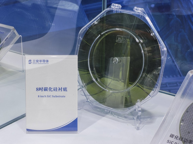
Several Chinese silicon carbide substrate manufacturers have recently disclosed progress in research, development, and early shipment of 8-inch conductive substrates, signaling that third-generation semiconductor upstream materials are accelerating their transition from 6-inch to 8-inch generation. Industry observers broadly expect that, as vehicle manufacturers become increasingly sensitive to SiC inverter costs, 8-inch substrates will become the mainstream choice for automotive-grade power devices over the next two to three years. The localization of the physical vapor transport (PVT) equipment that makes this possible is therefore entering a critical volume window.
PVT: The Core Process for SiC Crystal Growth
Silicon carbide single crystals are typically grown using the physical vapor transport method. Inside a high-temperature graphite furnace, high-purity SiC source powder sublimates at roughly 2,300 to 2,500 degrees Celsius, and the gaseous species deposit and crystallize on a cooler seed crystal. The entire process places extreme demands on radial temperature uniformity, the service life of graphite insulation felt, sealing integrity, and growth atmosphere control. A single boule can take several days or even more than a week to grow, and each run can cost hundreds of thousands of yuan. The stability of the furnace directly determines boule yield, dislocation density, and the number of usable wafers that can be cut from it.
The Engineering Challenges of Moving to 8 Inches
Scaling from 6 inches to 8 inches enlarges the thermal field diameter inside the furnace, making the radial temperature gradient much harder to control. This can easily introduce polytype inclusions, micropipes, and basal plane dislocations. International leaders required many iterations to achieve stable 8-inch growth. Chinese equipment makers, meanwhile, have made continuous breakthroughs in thermal field simulation, zoned temperature control, semi-automated seed and boule handling, and poly-source recycling. Domestic PVT furnaces are not only clearly cheaper than imported equipment but also offer shorter delivery times and responsive local service, and they are beginning to enter substrate fab lines in volume.
Market Outlook and Capacity Pace
Demand for SiC devices continues to expand as 800-volt vehicle platforms and photovoltaic inverters adopt SiC solutions, and substrates account for the largest share of device cost. Domestic substrate makers plan to bring 8-inch lines online over the next two years, driving concentrated procurement of PVT furnaces and associated hot-zone consumables. At the same time, 6-inch substrates will continue to serve industrial and photovoltaic inverter markets for a long time, so investment is running in parallel rather than as a clean switch.
Market Size and Demand Drivers
The global SiC device market is projected to keep a double-digit compound growth rate over the next several years, driven primarily by electric vehicle traction inverters, on-board chargers, and fast charging piles, with secondary contributions from photovoltaic inverters, rail transit, and industrial motor drives. Because the substrate represents roughly half the cost of a SiC device, any step toward larger-diameter, higher-yield substrates flows directly into device economics. Automakers are increasingly specifying SiC content across their high-voltage vehicle platforms, which pulls long-term offtake agreements and gives substrate makers the confidence to commit capital to 8-inch lines. For Chinese producers, the combination of growing domestic EV demand and a policy push toward supply-chain self-reliance creates a uniquely favorable backdrop for capacity build-out.
Technical Detail of the PVT Furnace
A modern PVT reactor consists of a water-cooled stainless-steel chamber, an insulated graphite hot zone, a graphite crucible holding the SiC source, and a seed crystal mounted at the top. Induction or resistive heating raises the source to sublimation temperature while the seed is held slightly cooler, establishing the temperature gradient that drives vapor transport upward. Crucial engineering parameters include the axial and radial temperature profile, growth rate, rotation rate, and chamber pressure, all of which influence polytype stability (4H versus 6H), residual stress, and defect density. Domestic furnace makers have made rapid progress in multi-zone heating, real-time temperature monitoring, and automated boule extraction, which collectively improve repeatability and reduce the per-run cost of consumables such as graphite felt and crucibles.
Outlook for the Coming Years
Looking ahead, the competition in 8-inch SiC substrates will be decided by crystal cost, yield, and the localization rate of supporting equipment. With 800-volt platforms and photovoltaic demand expanding, substrate capacity will keep growing. Domestic players that build an integrated capability spanning PVT growth, slicing, polishing, and cleaning will be best positioned in the global supply chain. For emerging substrate fabs, choosing a cost-effective and responsive domestic equipment partner is key to shortening ramp-up and controlling capital expenditure. The next two to three years will likely determine which Chinese substrate makers become volume suppliers to global device customers.
Cost Structure of SiC Substrates
The cost of a SiC substrate breaks down into crystal growth, multi-wire sawing, grinding, polishing, cleaning, and inspection. Crystal growth dominates because each PVT run consumes significant electricity, high-purity source powder, and consumable graphite parts, while yield loss is expensive at this stage. Slicing with diamond wires is the next major cost, and improving wafer thickness uniformity and kerf loss directly affects material utilization. Polishing and chemical mechanical steps must produce damage-free surfaces for epitaxy. Because every step compounds cost, improving growth yield and localizing consumables have a larger impact on final substrate price than optimizing any single step. This is why integrated domestic suppliers spanning growth and back-end processing hold a structural cost advantage.
Back-End Equipment Is Just as Critical
Once the boule is grown, it must go through orientation, sawing, grinding, polishing, cleaning, spin drying, and inspection before it becomes an epitaxy-ready substrate. Hebei Zhongke Microelectronics Co., Ltd., located in Fuxing District, Handan, Hebei Province, focuses on localizing semiconductor wafer and substrate back-end equipment. Its product line includes a VGF crystal growth furnace for compound semiconductors such as indium phosphide and gallium arsenide, a wafer unloading table, a fully automatic single-wafer cleaning machine, a single-wafer cleaning and spin dryer (model SG-8-12-2D), and wafer inspection lamps (QG-150/QG-250). These products allow substrate makers to build a coordinated chain from crystal growth through wafer cleaning, spin drying, and visual inspection, reducing dependence on imported equipment and shortening line ramp-up time.
As 8-inch SiC lines come online, coordinated localization of growth furnaces and back-end cleaning and drying equipment will become the main lever for cost reduction. To learn about VGF crystal growth furnaces, wafer unloading tables, and cleaning and drying solutions, call the consultation hotline: 17177768881.