
In compound semiconductor crystal preparation, Czochralski (CZ) pulling and vertical gradient freeze (VGF) are the two mainstream crystal growth routes. As demand for materials such as indium phosphide and gallium arsenide has grown, the industry has increasingly favored gradient freeze methods. Why is that, and what are the differences between the two approaches in thermal field, thermal stress, and defect control?
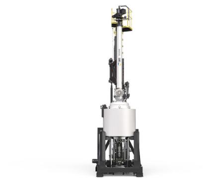
Czochralski: Classic but With Higher Thermal Stress
The Czochralski method pulls a seed crystal upward while rotating it from the melt, crystallizing progressively at the solid-liquid interface to produce a boule of controlled diameter. The equipment is mature and growth is fast, which is why it has long dominated silicon single crystals and some GaAs boules. However, during pulling, crystal rotation combines with melt convection, producing larger radial and axial temperature gradients that easily introduce dislocations and thermal stress. For volatile materials such as indium phosphide, which contains phosphorus with high vapor pressure at temperature, melt composition can drift and requires strict liquid encapsulation and pressure control. CZ also consumes crucibles and hot zones relatively quickly.
VGF: The Advantages of Gradient Freeze
In VGF, polycrystalline charge is sealed in a quartz ampoule, and the melt is solidified progressively from the seed end by lowering a temperature zone or moving a heater. Because the crystal is nearly stationary and the temperature gradient is gentle, thermal stress inside the boule is much lower, and dislocation density can be held to a very low level, which is especially suitable for defect-sensitive materials such as InP and GaAs. VGF also delivers higher boule yield and lower equipment maintenance cost, and the sealed ampoule effectively suppresses phosphorus and arsenic evaporation, making it the mainstream process for large-diameter InP and GaAs growth.
Where Each Process Fits
CZ remains widely used for pulled silicon crystals and large-diameter GaAs, thanks to fast growth and flexible diameter control. VGF, meanwhile, holds the advantage for low-dislocation InP and semi-insulating GaAs substrates used in optoelectronics. In practice, manufacturers often configure both types of equipment on the same site to cover different product requirements, choosing a route based on device requirements for substrate defect density, cost, and size rather than on dogma.
Defect Physics and Why It Matters
The practical difference between CZ and VGF shows up in the defect budget. In CZ, the combination of crystal rotation and steep axial gradients generates significant thermal stress that can multiply threading dislocations, which in turn degrade the leakage current and reliability of devices built on the wafer. VGF, with its gently moving isotherms and stationary crystal, minimizes thermally induced stress and yields boules with much lower dislocation density. For optoelectronic devices such as laser diodes, even a small density of dislocations can shorten operating lifetime, which is why material buyers specify dislocation counts per square centimeter and why VGF has become the default for InP and semi-insulating GaAs used in photonics and RF.
Equipment Cost and Operational Trade-offs
CZ furnaces are mature and widely available, and their higher growth throughput suits low-margin, high-volume silicon and large GaAs production. However, they consume crucibles and hot-zone parts faster and require tighter control of volatile species. VGF furnaces run slower per boule but offer better yield, lower consumable burn rate, and a simpler sealed-ampoule handling flow that reduces safety and contamination risks. For a new entrant, the total cost of ownership depends less on the sticker price of the furnace and more on boule yield, wafer usable area, and the ability to run stable processes without constant manual intervention, which is where modern domestic VGF systems have made the most visible improvement.
Outlook for Process Choice
Going forward, compound crystal growth will remain a mix of Czochralski and VGF, with different materials favoring different routes. As optoelectronic and power devices demand ever-lower substrate defect density, VGF’s advantage in InP and GaAs will strengthen further. Domestic furnace makers must keep investing in thermal field simulation, ampoule design, and automated control to compete in high-end substrate growth equipment. The coordinated progress of process and equipment is the foundation of compound semiconductor industry upgrading, and firms that tie equipment development closely to customer process needs will win the next round. In practice, the choice between CZ and VGF is rarely ideological; it is driven by device requirements, cost targets, and the capability of the available equipment. As domestic furnaces mature, substrate makers gain more flexibility to optimize their mix rather than being locked into a single imported technology.
Process Parameters That Matter
Regardless of route, crystal growth success depends on a handful of tightly controlled parameters: axial and radial temperature gradient, growth rate, rotation rate, and the purity and stoichiometry of the melt. In CZ, too steep a gradient causes thermal stress and dislocations, while too shallow a gradient slows growth and raises cost. In VGF, the translation rate of the temperature zone must match the solidification front so that the crystal remains single-phase and free of inclusions. Modern furnaces use computer-controlled multi-zone heating and real-time monitoring to hold these parameters within narrow windows, and the ability to reproduce a validated recipe across many runs is what separates production-grade equipment from laboratory prototypes. Domestic furnaces have closed much of this gap in recent years.
Domestic Furnaces and Coordinated Breakthrough
Behind the choice of process route lies the capability of crystal growth furnace equipment. Whether CZ or VGF, both require precise temperature control, vacuum sealing, atmosphere management, and automated crystal extraction. Hebei Zhongke Microelectronics Co., Ltd., drawing on its semiconductor equipment expertise, offers a VGF crystal growth furnace targeting indium phosphide and gallium arsenide, together with back-end equipment such as a wafer unloading table, a fully automatic single-wafer cleaning machine, and a wafer spin dryer. These products help Chinese compound semiconductor makers localize equipment during process upgrades, shorten line debugging cycles, and lower long-term maintenance costs.
No process route is inherently superior; the key is the right match to the material and device requirements. To learn about VGF crystal growth furnaces and the accompanying wafer unloading, cleaning, and drying equipment, call the consultation hotline: 17177768881.