
The third-generation semiconductor capacity expansion wave continues to build. Domestic SiC substrate makers have recently disclosed mass delivery progress for 8-inch conductive substrates, and the 6-inch to 8-inch transition has moved from the R&D stage into volume supply, making the cost-reduction path for automotive SiC devices much clearer.
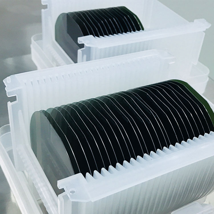
The Inevitable Move From 6 to 8 Inches
Silicon carbide substrates are the foundation of SiC MOSFETs, diodes, and other power devices. An 8-inch substrate yields roughly eighty percent more chips per wafer than a 6-inch substrate, which is the most direct lever for reducing automotive SiC device cost. As 800-volt EV platforms spread, SiC inverters are highly cost-sensitive, so substrate makers are focusing on 8-inch as their next-generation product. International leaders have already launched 8-inch samples, and Chinese makers are catching up fast.
Domestic Substrate Makers’ Mass Production Pace
Several Chinese SiC substrate makers already stably mass-produce 6-inch substrates and have completed process development for 8-inch conductive substrates across boule growth, slicing, and polishing. Localized PVT growth furnaces are a key part of this: domestic furnaces compete on thermal control, source-powder utilization, and maintenance cost, underpinning rapid capacity expansion. Key metrics such as dislocation and micropipe density continue to approach international first-tier levels, with some products passing downstream device qualification and entering small-batch supply.
Substrate Yield and Cost Metrics
SiC substrate cost and yield depend mainly on boule utilization, dislocation density, and processing loss. Although 8-inch substrates yield more chips per wafer, controlling polytype inclusions, micropipes, and basal dislocations during growth is harder. Domestic makers improve dislocation density through better PVT hot zones, optimized seed orientation, and disciplined dicing, grinding, and cleaning. Localization of wire saws and polishing also lowers processing cost. In cost-sensitive automotive applications, every percentage-point gain in substrate yield meaningfully improves device maker profitability.
Device Adoption and Market Pull
The move to 8-inch SiC is ultimately driven by device makers' need to lower the cost per ampere of current handling. SiC MOSFETs and Schottky diodes are displacing silicon IGBTs and diodes in main inverters of premium electric vehicles, where efficiency gains translate directly into extended range. As automakers broaden SiC adoption from high-end models to mass-market platforms, volumes ramp and the incentive to use 8-inch substrates grows accordingly. Charging pile operators and industrial inverter makers are secondary pull factors. For substrate manufacturers, signing long-term supply agreements with device customers is what justifies the heavy capital cost of new 8-inch crystal growth and processing lines.
Defect Density and Qualification
SiC substrates are graded by micropipe density, basal plane dislocation density, and other structural defects, and device fabs reject material that exceeds their limits. Achieving low defect counts at 8 inches is harder because the larger boule is more prone to temperature non-uniformity during growth. Domestic substrate makers have invested in improved PVT hot-zone design, seed selection, and post-growth characterization to bring defect levels into the acceptable range. Qualification at a device customer typically takes many months of lot-by-lot validation, which is why the transition from sample to mass delivery is a meaningful milestone rather than a formality.
Outlook for SiC Substrate Volume
Looking ahead, SiC substrates will accelerate from 6-inch mature supply toward 8-inch as the downstream application base broadens from premium EVs to mass-market vehicles and industrial uses. As device costs fall, demand will widen. Substrate makers expanding capacity will strongly demand localized growth furnaces, slicing, grinding, polishing, cleaning, and inspection equipment. Domestic equipment suppliers that can deliver high-purity, low-damage back-end processing will directly help SiC substrate makers raise yield and cut cost per wafer, sharing in the third-generation expansion dividend. Because SiC is hard to machine, every back-end step must be carefully controlled to avoid subsurface damage that later degrades epitaxy and device performance. This makes specialized cleaning, spin drying, and visual inspection equipment not an afterthought but a core part of substrate cost and yield. Domestic suppliers that understand SiC’s particular handling needs will win share as 8-inch lines come online. Because SiC device demand is tied to vehicle production, the substrate expansion is expected to track EV sales growth closely, giving well-positioned suppliers a multi-year demand runway. Backing that demand with localized cleaning, spin drying, and inspection equipment reduces both capital cost and long-run maintenance burden for substrate makers. As 8-inch SiC becomes the volume platform of the next decade, the substrate makers that pair cheap, stable growth with clean, precise back-end processing will define the cost structure of the whole SiC device industry. For device makers, cheaper, more available substrates directly translate into more affordable EVs, which in turn broadens the demand base further, creating a virtuous cycle of volume and cost reduction.
Where SiC Devices Are Used
SiC power devices are most valuable where high voltage, high frequency, and high temperature coincide. The dominant application is the EV main inverter, where SiC MOSFETs raise efficiency and extend range, followed by on-board chargers, fast charging piles, and photovoltaic inverters. Industrial motor drives and rail traction are secondary markets. As SiC device prices fall, adoption spreads from premium vehicles to mass-market platforms, which multiplies volume and pulls substrate demand. Device makers rely on predictable substrate supply to plan their fab utilization, so they increasingly sign multi-year agreements with qualified substrate producers, giving those producers the revenue visibility needed to invest in 8-inch lines and supporting equipment.
Back-End Cleaning, Drying, and Inspection
SiC is extremely hard, so slicing, grinding, and polishing introduce significant particles and surface damage that place high demands on subsequent cleaning, spin drying, and inspection. Hebei Zhongke Microelectronics Co., Ltd. offers, for third-generation substrate back-end processes, a wafer unloading table, a fully automatic single-wafer cleaning machine, a 12-inch wafer spin dryer (SG-8-12-2D), wafer inspection lamps (QG-150/QG-250), and vacuum tweezers (PT-02/PT-04). These help SiC substrate makers achieve high-purity, low-damage processing during boule and wafer handling, reducing yield loss from particle contamination.
As 8-inch SiC substrates enter mass delivery, they will drive coordinated localization across the entire third-generation line. For inquiries about wafer cleaning, spin drying, unloading tables, and inspection equipment, call the consultation hotline: 17177768881.