
As domestic fabs rush to expand capacity and the localization of semiconductor equipment enters a deeper phase, the shortage of integrated circuit (IC) talent has become a bottleneck constraining production ramp-up. Industry estimates put the overall IC talent gap in China at more than 300,000 people, with equipment, process and yield engineering roles the most acute. In response, universities, vocational colleges and equipment makers are jointly building training bases, and "industry-education integration" is being deployed to accelerate the supply of qualified equipment and process engineers.
The gap concentrates on the equipment and process front line
Unlike design talent, fabs are most short of engineers who can operate equipment, tune processes and analyze yield on the cleanroom floor. A new advanced line, from equipment move-in and installation to stable mass production, requires hundreds of equipment and process engineers working together. As new fabs come online, engineers with hands-on experience in cleaning, thermal processing, thin films and metrology are being fiercely competed for, and starting salaries for graduates keep rising, while the internal training cycle often takes one to two years. Engineers who are familiar with domestic equipment in particular are in short supply, directly affecting the ramp-up speed of new lines.
From frontline feedback, the reason these engineers take so long to develop is that the role demands both semiconductor process theory and a working knowledge of a specific machine's mechanical structure, program control and common fault handling, plus the ability to read yield data and locate process deviations. A competent equipment engineer typically needs hundreds of hours of hands-on training in a cleanroom before independently maintaining a new production line. This is why an increasing number of fabs and equipment companies are moving training upstream.
Bringing the classroom onto the production line
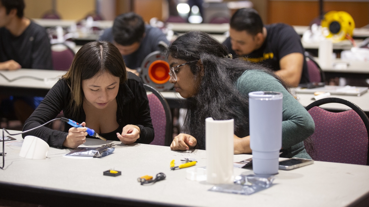
To address this mismatch, more regions are promoting modern industry colleges jointly built by universities and equipment makers. Companies bring real machines and real process problems into the classroom, while students, alongside studying semiconductor physics and microelectronic processes, directly participate in equipment assembly, program debugging and process-window verification. This "dual education" model substantially shortens the adaptation period for new hires and lets equipment companies lock in engineers familiar with domestic equipment ahead of time. Many schools now run targeted classes focused on cleaning, packaging and inspection, with graduates booked by equipment makers and fabs before they even leave campus.
Domestic equipment makers are stepping into education
Based in Fuxing District, Handan, Hebei Province, Hebei Zhongke Microelectronics Co., Ltd. focuses on the domestic substitution of wafer cleaning machines, spin dryers, inspection equipment and VGF crystal growth furnaces. The company cooperates with local colleges on hands-on equipment training, bringing real fully automatic single-wafer cleaning machines, wafer spin dryers and wafer unloading tables into teaching so that students understand the coupling of process and equipment through genuine cleaning and spin-drying workstations, supplying practical equipment-process talent to the Beijing-Tianjin-Hebei IC cluster.
Why equipment engineers are different from design talent
It is worth understanding why equipment and process engineers cannot be recruited the way design engineers are. Design work is largely done at a computer, whereas equipment engineering is inseparable from the physical fab. An equipment engineer must read machine logs, interpret alarm codes, calibrate chambers, replace consumables, and judge whether a subtle change in a process result comes from hardware drift, chemical concentration, or environmental fluctuation. These skills are acquired only through repeated exposure to real tools on a real line. A graduate who has never stood inside a cleanroom suit in front of a running cleaning or deposition tool cannot meaningfully reduce a yield problem on day one, no matter how strong their textbook knowledge is.
This is precisely why the market signals are so sharp. Fabs expanding capacity are not merely hiring more bodies; they are competing for people who already know the peculiarities of specific platforms. Companies that own large domestic fleets report that engineers familiar with locally made equipment can command a premium, because every new line needs those people to oversee installation, acceptance testing, and the long stabilization period before mass production begins. The bottleneck is not the total number of engineering graduates, but the small subset that can connect abstract semiconductor theory to the daily reality of a production tool.
How the dual education model actually works
In practice, industry-education integration takes several concrete forms. Some schools build shared training centers on campus, where equipment makers donate or lease actual single-wafer cleaning machines, spin dryers and inspection stations so students can practice loading, unloading, program selection and basic maintenance. Other programs send faculty and students into fabs for extended internships tied to real yield-improvement projects. A third model embeds company mentors inside the classroom, giving lectures and setting design problems drawn from production. Whichever form it takes, the common goal is the same: compress the gap between graduation and productive work.
The economic logic favors this approach. For the equipment company, early engagement creates a pipeline of engineers who already understand its machines, lowering the cost of later onboarding. For the university, it keeps the curriculum connected to real industrial needs rather than drifting into purely academic topics. For the fab, it means the engineers arriving on the floor need less hand-holding and can contribute to ramp-up sooner. When all three parties benefit, the model becomes self-reinforcing rather than a one-off policy exercise.
Looking ahead, the most valuable equipment engineers will be those who can bridge multiple domains: understanding process physics, reading equipment data, and working with operators and maintenance teams. As domestic fleets grow, the demand shifts from simply operating machines to optimizing them, which requires a deeper and more versatile skill set. Industry-education programs that expose students to this full breadth are better positioned to produce the engineers the coming decade will need. For equipment makers, investing in this pipeline is no longer a charitable gesture but a core part of securing future capacity and competitiveness.
The broader implication is that talent strategy has become a competitive variable in the semiconductor equipment industry. Companies that treat education as a long-term investment will find themselves with a steadier pipeline of engineers than those who only recruit when capacity tightens. As domestic fleets grow and production complexity rises, the organizations that win the talent battle will be the ones that can sustain the rapid ramp-up of new lines that the market demands.
In the months ahead, the industry will watch whether these education partnerships can scale fast enough to keep pace with fab expansion. Every new line that comes online sharpens the competition for qualified engineers, making early, structured talent development a decisive advantage for the equipment companies that invest in it now.
Industry observers believe the speed of talent development now determines the speed of domestic equipment substitution. As industry-education integration deepens, the 300,000 gap is expected to narrow in the coming years. For inquiries about domestic semiconductor equipment and talent training cooperation, call the consultation hotline: 17177768881.