
A new round of policy momentum is driving coordinated development of integrated circuits across the Beijing-Tianjin-Hebei region. The supporting three-year action plan has now been formally rolled out, defining a division of labor: Beijing strengthens design and equipment R&D, Tianjin focuses on packaging, testing and advanced manufacturing, and Hebei develops specialty processes and materials leveraging its resources and manufacturing base. Hebei is emphasizing compound semiconductors as a differentiated track, avoiding homogeneous competition with the Yangtze River Delta.
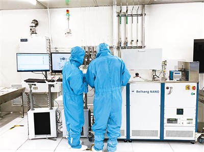
Three regions, differentiated roles
The Beijing-Tianjin-Hebei area is rich in universities, research institutes, equipment and design resources, but has long suffered from weak industrial coordination. The new plan takes a clustered approach: Beijing relies on universities and its headquarters economy for IC design and high-end equipment R&D; Tianjin uses its port and manufacturing base for packaging, testing and specialty lines; and Hebei applies its land, energy and location advantages to focus on silicon carbide, gallium nitride and indium phosphide (InP) compound semiconductor devices and related equipment, providing nearby support for regional new-energy vehicles, photovoltaics and power electronics.
Hebei plays the compound semiconductor card
Compound semiconductors are in strong demand for power devices, radio frequency and optoelectronics, and depend less on the most advanced nodes, making them a natural fit for Hebei's manufacturing and cost advantages. With policy support, a number of substrate-epitaxy, device manufacturing and specialty equipment projects are landing in Hebei, driving synchronized growth in local semiconductor equipment, cleanroom facilities and inspection suppliers, and gradually forming a specialty chain from materials and devices to dedicated equipment. Handan and Shijiazhuang are also planning specialty parks for power devices and dedicated equipment to absorb research achievements spun out from Beijing and Tianjin.
Specialty equipment gains matching opportunities
Hebei Zhongke Microelectronics Co., Ltd., based in Fuxing District, Handan, is one such equipment supplier within this specialty cluster. The company makes fully automatic single-wafer cleaning machines, InP cleaning machine model SQX-150-5Y1D, wafer spin dryers, EFEM cleaning & drying systems and wafer unloading tables, providing domestic solutions for cleaning, spin-drying and inspection on compound semiconductor and specialty lines, serving the Beijing-Tianjin-Hebei wafer manufacturing cluster nearby and helping fabs cut dependence on imported equipment.
Why compound semiconductors fit Hebei's position
Compound semiconductors differ from mainstream silicon logic in an important way: they are less dependent on the most advanced lithography nodes. Power devices made of silicon carbide or gallium nitride, radio frequency chips built on gallium nitride, and optoelectronic devices based on indium phosphide all demand precision and clean manufacturing, but they do not require sub-seven-nanometer scaling. This makes them a natural arena for a region that is building its industrial base rather than trying to match the leading-edge logic fabs concentrated elsewhere. It also means the value chain is more accessible to local equipment and materials suppliers, who can participate without mastering the absolute highest-end processes.
For Hebei, the strategic bet is that by focusing on this differentiated track it can avoid a costly race to replicate what the Yangtze Delta and the Bohai Rim cities already do well. Instead, it can build a reputation as a home for compound device fabs and the specialized equipment that serves them. The spillover effects are meaningful: a device fab needs gas and chemical supply, cleanroom facilities, wafer cleaning and spin-drying tools, inspection stations, and packaging support, all of which can be sourced locally if the ecosystem is nurtured. Over time this creates a cluster where companies serve one another, reduce logistics and coordination costs, and share a common talent pool.
What the three-year plan actually changes
The action plan is more than a statement of intent. It coordinates investment in parks, clarifies which type of project each city should pursue, and encourages the transfer of research results from Beijing's universities into production in Tianjin and Hebei. Practical measures include streamlined approval for specialty fab projects, support for shared pilot lines, and funding for the training needed to staff these lines. For equipment makers, the plan translates into a more predictable regional market: instead of guessing where the next compound device project will land, suppliers can align their product roadmaps with the declared direction.
Regional coordination also reduces waste. Without a plan, neighboring cities might each attempt to build the same kind of line, splitting demand and leaving everyone subscale. The division of labor means Beijing concentrates on design and research, Tianjin on manufacturing and packaging, and Hebei on specialty devices and equipment that feed into the whole supply chain. The result is a more efficient allocation of capital and a stronger collective position in the national IC landscape.
The regional plan also carries implications for suppliers outside the device fabs themselves. As compound device lines take shape, they pull demand for specialized cleaning, spin-drying and inspection tools that match the specific chemistry of materials such as silicon carbide and indium phosphide. Local equipment makers that understand these processes can become preferred suppliers rather than afterthoughts. Over time, the goal is a self-reinforcing regional chain where device makers and equipment firms grow together, reducing reliance on distant imports and strengthening the overall resilience of the regional semiconductor industry.
For the region, the coming years will show whether the division of labor translates into tangible output. If the compound semiconductor track gains real project traction, Hebei will not only host new fabs but also nurture a stable base of equipment and materials suppliers, creating durable local employment and industrial capacity. That outcome would make the three-year plan a model for how a region can specialize rather than imitate, and carve out a defensible position in the national semiconductor supply chain.
The next phase will depend on turning policy intent into concrete fab and equipment projects. If the compound semiconductor track gains traction, it will strengthen not only Hebei's industrial base but the entire regional supply chain, demonstrating how coordinated specialization can secure a lasting role in the national semiconductor ecosystem.
As the three-year plan advances, the regional IC industry is expected to take shape through coordinated specialization, with Hebei's compound semiconductor track becoming an important growth pole. For line equipment matching inquiries, call the consultation hotline: 17177768881.