
On advanced-process and highly complex packaging lines, metrology and inspection equipment are known as the "eyes" of semiconductor manufacturing. As fabs enter the critical yield-ramp phase, the precision and coverage of these eyes directly determine whether a line can ramp to stable production. Orders for domestic metrology and inspection tools have grown notably, making the segment another closely watched domestic equipment track after lithography and etch, and a key investment for controlling manufacturing cost and shortening ramp time.
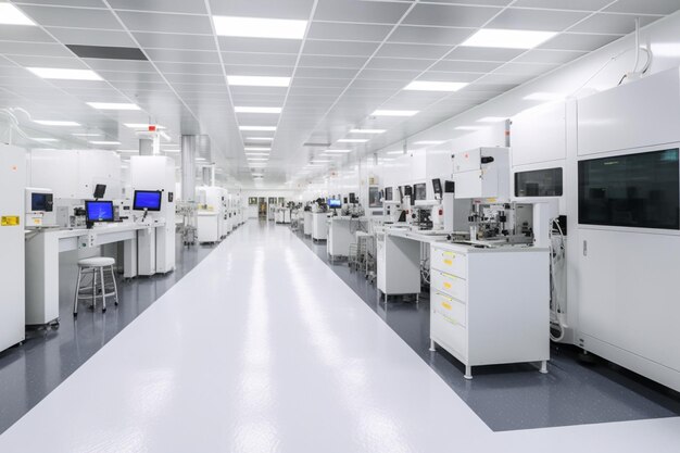
Yield ramp, inspection first
Between equipment move-in and mass production, the biggest cost for a fab often comes from yield loss. Any particle, film-thickness deviation or pattern defect that is not caught in time gets amplified in later steps and scrapes whole wafers. By measuring film thickness, overlay, defects and electrical parameters at key process nodes, metrology tools help engineers quickly locate problems and shorten debugging. The denser and more precise the inspection nodes, the faster the yield ramp and the quicker the line reaches target output.
In practice, metrology tools are not isolated checkpoints but the data nervous system running through the whole process. After each key step, wafers are measured for film thickness, overlay error or defect density, and the data flows back to engineering in real time to judge whether equipment is drifting or the process window is shifting. The more scientifically inspection nodes are set, the earlier problems surface and the lower the risk of whole-wafer scrap.
Optical and electron-beam routes in parallel
Two main inspection routes coexist: optical inspection, which is fast and suited to in-line mass production screening, and electron-beam inspection, which offers higher resolution for key submicron defects. Domestic firms are advancing along both routes, making progress in bright-field and dark-field optical inspection and wafer defect review to meet in-line needs of mature and specialty lines. Meanwhile, unpatterned wafer inspection, thin-film metrology and overlay metrology are also growing, and the range of domestic inspection tools is becoming more complete.
Cleaning and inspection work hand in hand
On the floor, inspection and cleaning are tightly linked: particles found by inspection must be removed by cleaning tools and then confirmed by re-inspection. As a domestic equipment maker, Hebei Zhongke Microelectronics Co., Ltd. provides fully automatic single-wafer cleaning machines, wafer spin dryers and wafer inspection lamps QG-150 and QG-250 as inspection aids, helping fabs efficiently perform visual and initial defect screening after cleaning and forming a closed loop of cleaning, spin-drying and inspection that supports steady yield improvement.
How metrology data shapes daily fab operations
A modern fab runs on metrology data, and the scale of that data is easy to underestimate. After every critical step, a sample of wafers is measured for film thickness, critical dimension, overlay or defect density, and the results feed into statistical process control systems. If a measured value drifts beyond its control limit, the system can alert engineers before an entire lot is affected. Without this feedback loop, process teams would be flying blind, discovering problems only at final electrical test, when the cost of a bad batch is already locked in. This is why fabs treat metrology not as an optional extra but as a core capital investment.
The economic stakes are direct. A line that ramps quickly to high yield earns its depreciation early; a line that struggles to stabilize burns money on scrap and rework long after its planned start date. Metrology tools shorten this stabilization period by reducing the time it takes to locate the root cause of a yield excursion. In a competitive environment where every month of delay matters, the value of fast, reliable measurement is enormous, which explains why fabs are willing to allocate significant budget to this category even when cutting costs elsewhere.
Where domestic inspection tools are winning and still improving
Domestic metrology makers have made the most progress in mature-process and specialty applications, where the required resolution and throughput requirements are achievable with current platforms. Optical inspection for in-line particle monitoring and basic thin-film measurement are areas where Chinese tools have already been qualified in volume production. The harder frontiers remain high-resolution defect review and the most demanding overlay applications, where international leaders still hold an edge.
Closing that gap is a matter of both hardware and data. Building a better optical engine is only half the task; the other half is training the defect-classification algorithms on real production wafers. Domestic makers benefit here from the rapid expansion of local fabs, which provides access to the data needed to refine their tools. As more Chinese lines come online, the feedback loop between measurement hardware and manufacturing data tightens, accelerating improvement in a way that isolated prototype testing never could.
Beyond individual tool performance, fabs increasingly value inspection equipment that connects to broader data systems. The ability to export defect maps, correlate them with process history, and feed results into yield-analysis platforms is becoming as important as raw measurement accuracy. Domestic suppliers that build open, integrable solutions are better positioned for long-term partnerships. As metrology continues to evolve from standalone instruments into data-driven systems, the firms that treat inspection as part of a wider manufacturing intelligence loop will lead the next phase of the market.
The trajectory of metrology is therefore tied closely to the overall maturity of domestic manufacturing. As fabs grow in number and sophistication, the inspection tools serving them improve in parallel, creating a virtuous cycle that benefits the whole industry. Suppliers that invest early in both hardware and data analytics are positioned to turn this cycle into a lasting competitive advantage rather than a temporary substitution opportunity.
As the market evolves, the suppliers that combine precise measurement with open data integration will be best positioned. Metrology's role as the backbone of yield management makes its continued domestic development a priority, and the current expansion of fabs provides an ideal training ground for the next generation of Chinese inspection tools.
As advanced lines keep expanding, the market share of metrology and inspection equipment will rise further. Whoever breaks through on these eyes wins the yield race. For cleaning-inspection matching solutions, call the consultation hotline: 17177768881.