
As the highest-barrier equipment in chipmaking, lithography has long been the summit of Chinese semiconductor equipment development. In recent years, domestic lithography tools have advanced steadily on mature nodes, with 28nm immersion DUV (deep ultraviolet) lithography now entering batch delivery, an important milestone from R&D to mass-manufacturing application, and a strong support for supply-chain security of domestic mature and specialty lines.
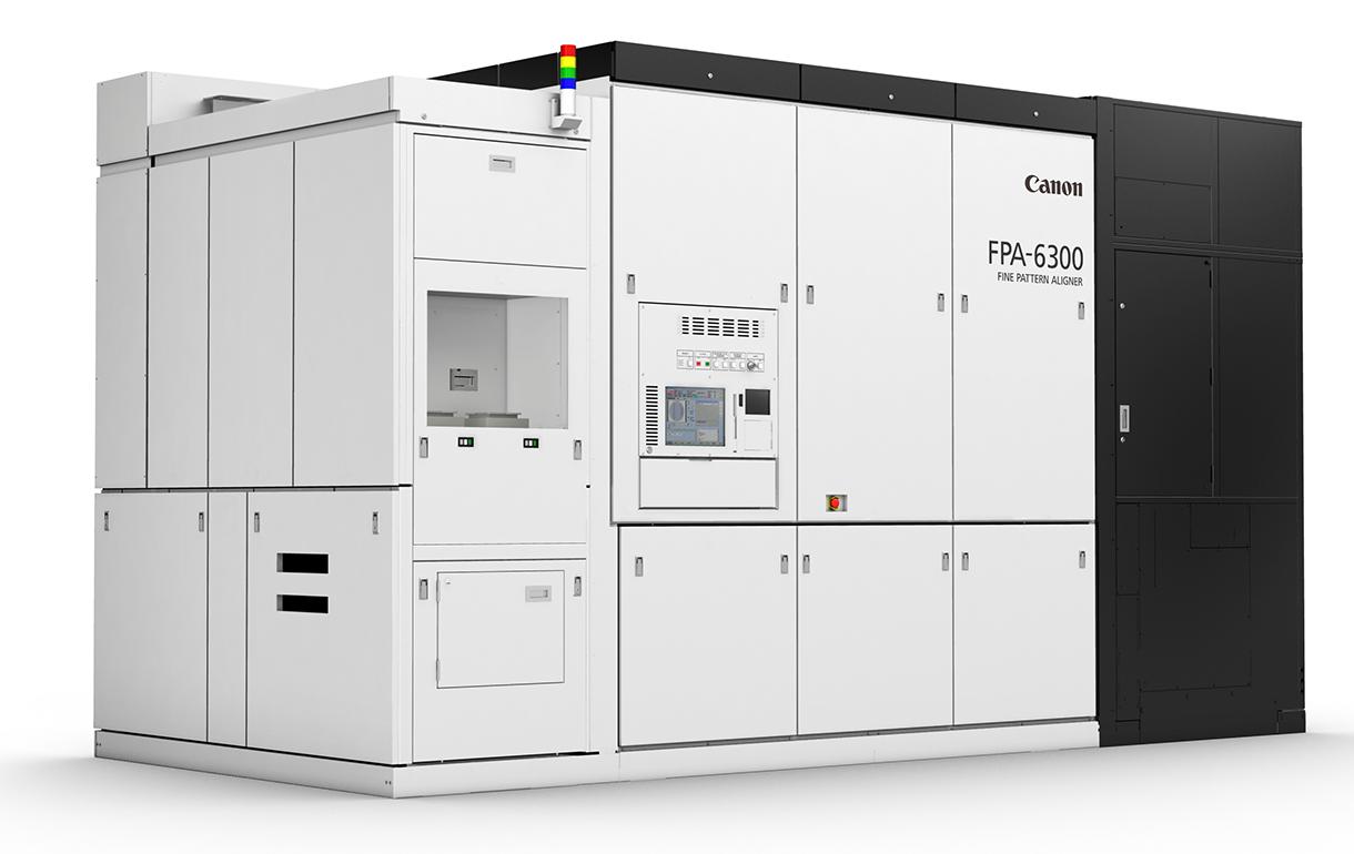
Lithography: the crown of chipmaking
Lithography transfers circuit patterns precisely onto the wafer, deciding minimum line width and integration density, and is the most complex and expensive step. A high-end scanner integrates optics, precision mechanics, motion control and environmental control, making its localization extremely hard. China has persisted in lithography investment, accumulating on scanning projection tools and conquering core subsystems from light source and objective lens to wafer stage, ultimately raising whole-machine capability step by step.
28nm immersion DUV in batch delivery
Immersion DUV raises resolution by filling liquid between the objective and wafer, and is the workhorse for mature and specialty lines. Recently, domestic 28nm immersion DUV lithography has entered batch delivery, marking a shift from single-unit validation to stable supply and the ability to build domestic mature-process lines. This progress matters for supply-chain security of specialty, power and analog chip lines and gives fabs more autonomous choice when buying key equipment.
From the market landscape, mature and specialty processes remain the realistic main battlefield where domestic lithography can first stand firm. Power devices, analog chips, automotive electronics and power-management chips do not rely on the leading edge yet enjoy large, growing demand, giving domestic immersion DUV broad application space. Reaching batch delivery at 28nm proves domestic lithography has scalable, repeatable production capability rather than a one-off research unit.
Lithography peripheral equipment goes domestic too
Lithography does not run alone; its front and back steps need matching cleaning, spin-drying, coater-developer and inspection tools. As a domestic equipment partner, Hebei Zhongke Microelectronics Co., Ltd. provides fully automatic single-wafer cleaning machines, wafer spin dryers and wafer inspection lamps QG-150 and QG-250, offering domestic wafer cleaning, drying and surface inspection for lithography lines, jointly building mature-process lines with domestic scanners.
Why mature-node lithography still matters
Much of the public conversation about lithography focuses on the most extreme leading-edge tools, but the real volume market for lithography lies in mature and specialty nodes. Power devices, analog circuits, automotive chips, display drivers and many radio-frequency components are manufactured on process generations measured in tens or hundreds of nanometers, not single-digit nanometers. These segments are large, growing steadily, and serve essential markets from electric vehicles to industrial control. Securing reliable lithography for these nodes is therefore strategically vital even apart from the race to the leading edge.
Batch delivery of a domestic 28nm immersion tool is significant precisely because it proves scalability. A working prototype in a laboratory is one thing; a machine that can be repeatedly delivered, installed and operated in volume production is another. It means the design is stable, the manufacturing process for the tool itself is repeatable, and service infrastructure can support a fleet. For a fab weighing supply-chain security, the ability to source a proven domestic scanner changes the risk calculus of long-term planning.
The ecosystem around a scanner
A lithography tool does not operate in isolation. Around it sits a supporting chain of coating and developing tools, cleaning and spin-drying equipment, metrology and inspection stations, and the carriers that move wafers between them. The performance of the total line depends on how well these surrounding steps prepare and verify each wafer. This is why the localization of lithography inevitably pulls along the localization of its adjacent equipment, and why domestic suppliers of cleaning, drying and inspection tools are important participants in this ecosystem rather than peripheral vendors.
For the Chinese semiconductor equipment industry, the steady progress of lithography is a marker of overall maturity. It signals that the hardest subsystem in chipmaking is being addressed with patience and long-term commitment. While the most advanced nodes remain a longer-term objective, the ability to serve mature and specialty volume production with domestic scanners is a concrete, valuable achievement.
It is also worth noting that progress in lithography depends on a deep ecosystem of optics, precision motion and control technology, all of which take years to mature. Batch delivery of a 28nm immersion tool reflects success across this whole supply chain, not a single breakthrough. For the Chinese equipment industry, this kind of systems-level achievement is a leading indicator of broader maturity. While leading-edge nodes remain a long-term objective, the ability to reliably serve the large mature-node market with domestic scanners is already delivering tangible value to the country's semiconductor supply chain.
The path forward for lithography will continue to balance ambition with realism: serving the large mature-node market reliably while investing steadily toward more advanced capability. Batch delivery of domestic immersion tools is a concrete milestone in that journey, proving that systematic, long-term engineering effort can translate into production-ready equipment. For the domestic industry, that proof is itself a valuable asset as it works to secure the equipment foundation of its semiconductor supply chain.
The coming years will show how quickly domestic lithography builds on this production milestone. Serving the large mature-node market reliably while advancing toward more capable tools is a balanced strategy, and the systems engineering proven by batch delivery gives the industry confidence in the road ahead.
For the Chinese supply chain, the value of a dependable domestic scanner for mature nodes is strategic even beyond leading-edge ambitions, since those nodes serve large and growing markets in power, analog and automotive chips.
This balanced approach to mature-node service and long-term advancement is what makes the current milestone both practically valuable and strategically significant.
The broader takeaway is that systematic, long-horizon engineering investment is paying off, and the domestic industry can build steadily on this production milestone toward ever greater capability.
Batch delivery of 28nm immersion DUV is a key step. With continued iteration, domestic lithography will hold mature nodes and accumulate ground for more advanced nodes. For lithography peripheral equipment, call the consultation hotline: 17177768881.