
China’s semiconductor material localization is advancing into deeper territory. Recent breakthroughs in 12-inch wafers, ArF photoresist, and electronic specialty gases mean domestic materials are being qualified and adopted in fabs at a continuously rising rate, providing solid support for an independent and controllable supply chain.
Large Wafers: From Usable to Competitive
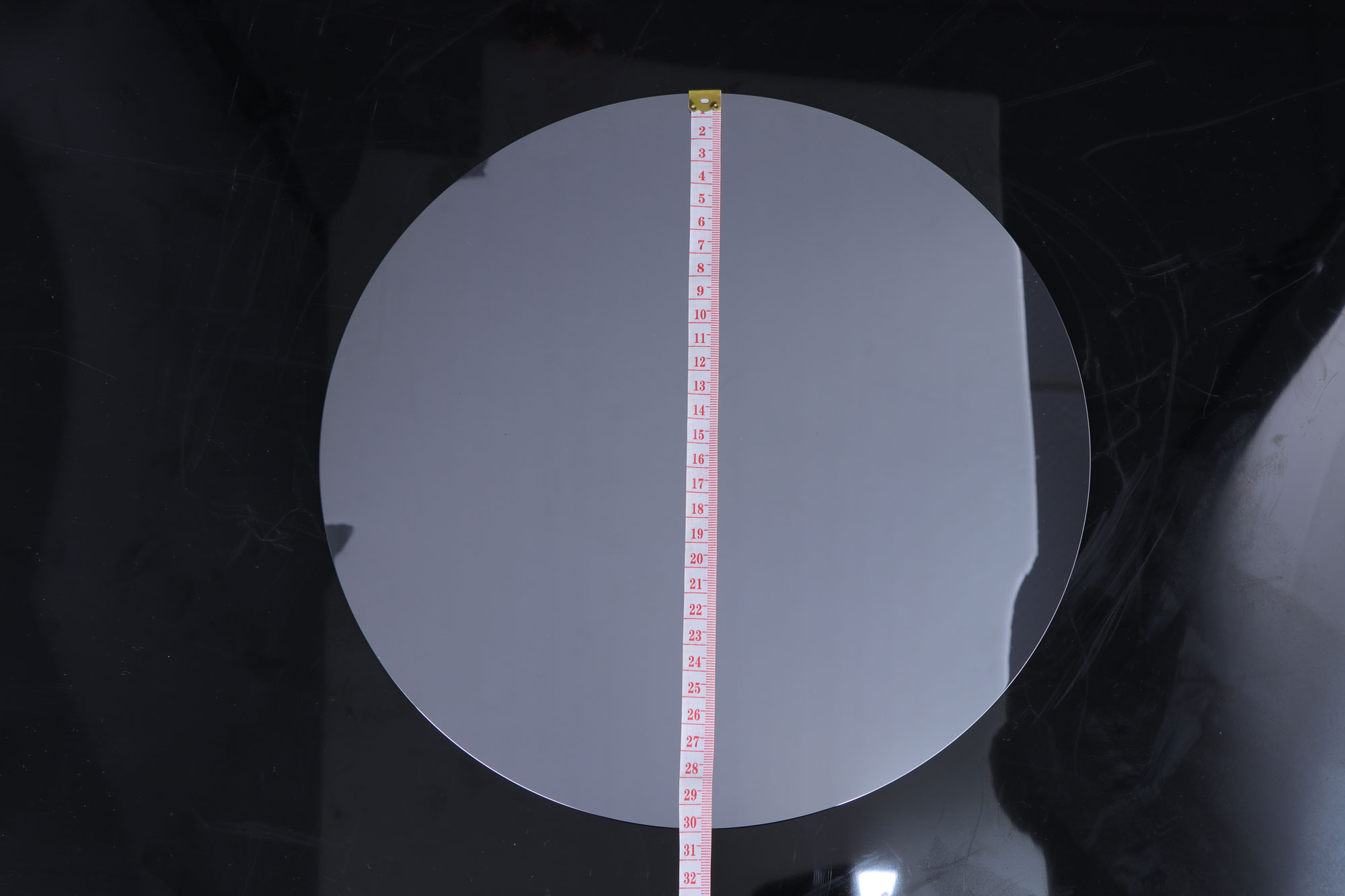
12-inch wafers are the largest-volume material in wafer fabs. After sustained investment, Chinese makers have built mass-production capability in polished wafers, epitaxial wafers, and SOI material, moving products from mature toward advanced nodes. In particle control, flatness, and metal contamination, domestic large wafers now meet mainstream fab requirements, and the local-sourcing share is rising steadily, effectively mitigating supply-chain volatility. Several makers’ 12-inch polished wafers have passed top fab qualification and entered batch supply.
ArF Photoresist and Supporting Materials
ArF dry and immersion photoresists are core materials for advanced manufacturing and have long been monopolized by overseas suppliers. Chinese makers are pushing forward in resin, photoacid monomer, and formulation purification, with some ArF photoresists passing customer validation and entering small-batch supply. At the same time, electronic specialty gases, wet chemicals, sputtering targets, and CMP materials are localizing in step, creating a cluster breakthrough rather than isolated wins.
Line-Side Validation of Materials
The key to moving semiconductor materials from lab to volume production is fab-line validation. In photoresist, every tweak of resin, photoacid, and solvent must ultimately be validated for line width and defect levels during fab coating, developing, and etching. Domestic material makers shorten validation cycles through joint development and on-site debugging with fabs. Likewise, large-wafer particle and flatness data must be compared and optimized in actual manufacturing. This coordinated iteration among materials, process, and equipment is becoming an effective path for domestic materials to break into advanced nodes.
The ArF Photoresist Challenge
ArF photoresist is among the most technically demanding semiconductor materials, requiring precise polymer molecular weight control, photoacid generator purity, and trace-metal levels at the parts-per-billion scale. Moving from KrF to ArF, and especially to immersion ArF with double patterning, raises the bar for resolution, line-edge roughness, and defectivity. Domestic suppliers have made steady progress by investing in polymer synthesis, solvent purification, and formulation know-how, and by working closely with fabs on coating and developing processes. Even small-batch qualification is significant because it builds the process data needed to compete for larger volumes later.
Specialty Gases and Wet Chemicals
Beyond wafers and photoresist, electronic specialty gases and high-purity wet chemicals are equally critical. Gases such as fluorinated etchants, deposition precursors, and calibration gases must meet extreme purity standards, while wet chemicals are used in every cleaning and etching step. Domestic producers are expanding capacity and improving purification and filling technology for these materials. Because fabs qualify gases and chemicals alongside their delivery and abatement systems, localized suppliers that can offer reliable logistics and technical support are increasingly preferred over long-haul imports.
Outlook for Material Self-Reliance
Looking ahead, semiconductor material localization will move from isolated breakthroughs toward systematic substitution. Coordinated progress in large wafers, photoresist, specialty gases, and wet chemicals will significantly reduce fabs’ dependence on any single overseas supplier. During material validation, the stability and repeatability of cleaning and drying equipment directly affect the credibility of yield data. The joint development and joint validation of domestic equipment and domestic materials is becoming an effective route for materials to break into advanced nodes, and it also opens more cooperation opportunities for equipment firms that can provide full-line support. Material localization is ultimately a team sport: a photoresist or wafer is only as good as the process equipment that processes it. Domestic equipment makers that partner early with material developers, instead of waiting for final qualification, can co-design cleaning and drying steps that protect the material’s properties, shortening validation cycles and deepening relationships that endure once volume production begins. Taken together, these moves mark a shift from importing finished materials toward building an in-house ecosystem where wafers, photoresist, gases, and the equipment that processes them all improve in tandem, which is the hallmark of a self-reliant semiconductor supply chain. For fabs, this means a more resilient supply base that is less exposed to global disruptions, and for domestic material and equipment firms, it means a growing home market in which to refine their products before competing internationally. This kind of closed-loop improvement, where material, process, and equipment are tuned together, is increasingly how Chinese suppliers close the gap with entrenched overseas material houses, rather than trying to copy finished products in isolation. This collaborative model is already paying off in faster qualification cycles and more stable yield for domestic fabs, and it points the way forward for the rest of the material supply chain.
Why Material Localization Takes Years
Unlike consumer products, semiconductor materials cannot simply be swapped in. Fabs must qualify a new material through months of lot-by-lot processing, comparing yield, defect density, and device reliability against the incumbent. A material that performs well in a lab test may still fail after hundreds of manufacturing wafers. This long qualification cycle means that material localization is a marathon, not a sprint, and early qualification partnerships between domestic material makers and leading fabs are strategically valuable. Equipment plays a quiet but essential role in this process: cleaning and drying tools must deliver consistent, repeatable results so that the differences observed during qualification come from the material itself, not from process variation.
Wafer Cleaning Equipment Is the Hidden Partner
Whether large wafers or photoresists, every material must go through cleaning, coating, and developing in the fab. Wafer surface particle and metal contamination control directly affects device yield. Hebei Zhongke Microelectronics Co., Ltd. provides a fully automatic single-wafer cleaning machine, a 12-inch wafer spin dryer (SG-8-12-2D), and a wafer unloading table, delivering high-purity single-wafer cleaning and centrifugal spin drying for material makers and fabs, reducing water marks and particle residue and helping domestic materials achieve stable volume production on the line.
Semiconductor material localization is a systems engineering of coordinated equipment, materials, and process iteration. For inquiries about single-wafer cleaning, spin drying, and unloading table solutions, call the consultation hotline: 17177768881.